PCB Design, Assembly, and Fabrication
Printed Circuit Board (PCB) design involves far more than meeting basic functionality requirements. Every component, from tiny chips to intricate circuits, carries specific requirements and functions that significantly impact efficiency, lifespan, manufacturing costs, market regulations (such as lead compliance), firmware integration, and complexities arising from mixed technologies. With extensive experience and expertise, KAI Engineering guides you through each critical decision. Our U.S.-based, in-house engineering team specializes in quickly and accurately prototyping your PCB, developing firmware, and managing all complexities associated with manufacturing—often known as Design for Manufacturing (DFM).
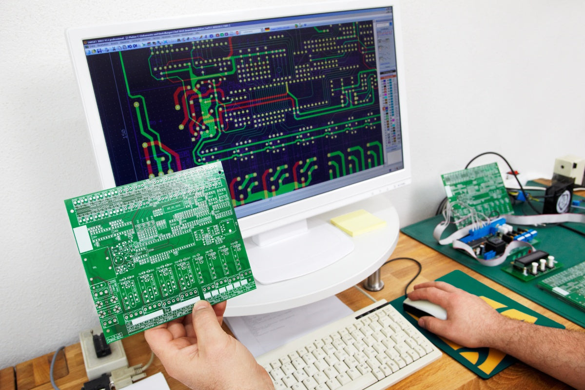
Schematic Capture and Layout
Schematic capture is a critical phase within the Electronic Design Automation (EDA) process. During this stage, our in house designers meticulously create electronic diagrams or schematics, forming the foundational blueprint for your product's electronic systems
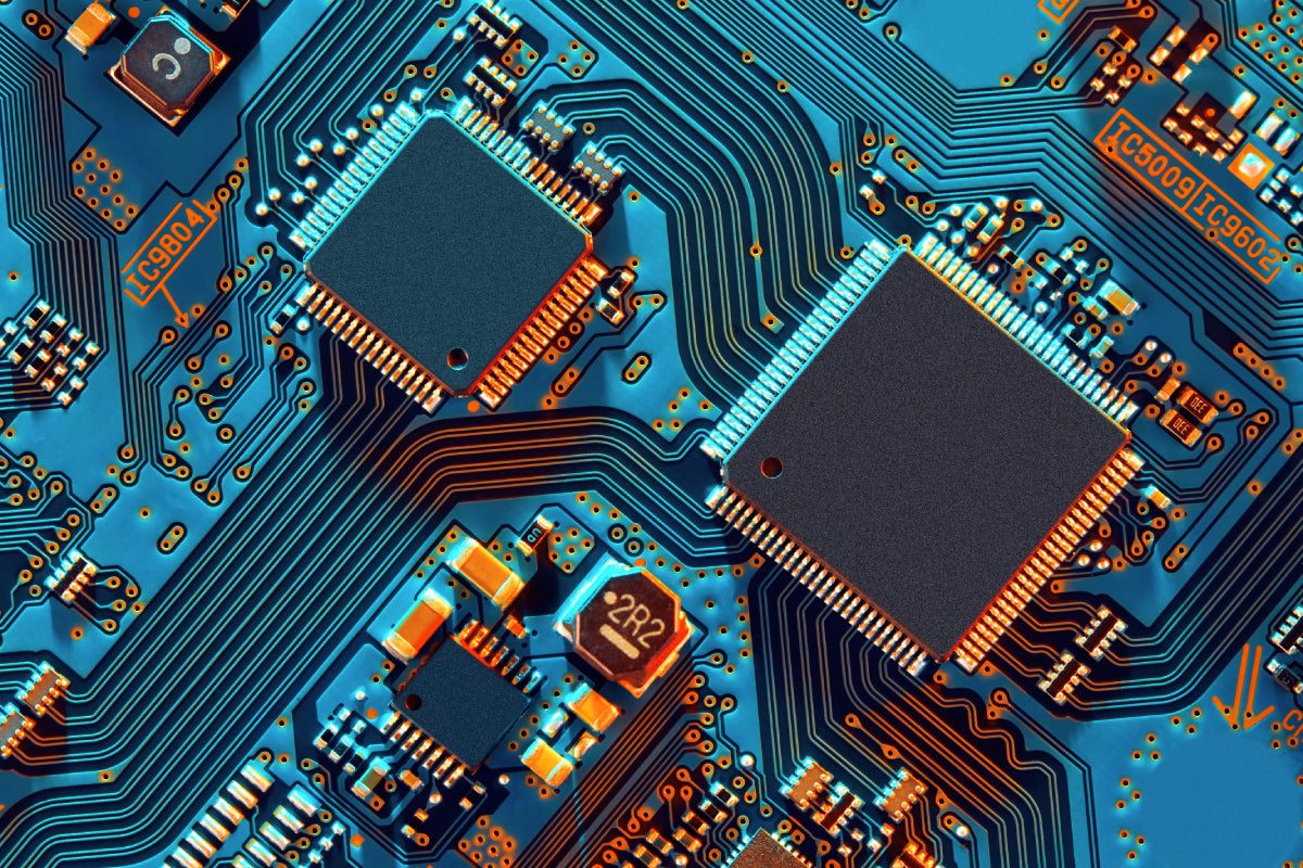
PCB Fabrication
Our skilled engineers then meticulously build the circuit board based on detailed schematic designs, ensuring precision, reliability, and optimal performance.
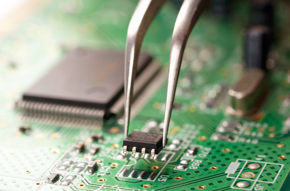
PCB Assembly
Known as Printed Circuit Board Assembly (PCBA), this process involves carefully mounting electronic components onto the PCB. The PCB provides mechanical support and connections for these components, while the components themselves deliver the required functionality.
Test and Inspection
Testing and inspection of PCB boards vary greatly depending on factors such as purpose, complexity, and manufacturing considerations (Design for Manufacturing - DFM). At KAI Engineering, our comprehensive testing and quality inspection processes ensure every PCB meets performance and reliability standards, safeguarding the success of your product.
One Week Quick Turn-Around for PCB and PCBA
Our team of highly experienced U.S.-based engineers and advanced, high-tech production facilities ensure fast turnaround times and rapid prototyping, delivering accurate, high-quality results quickly.
Pre-testing for UL, FCC, CE and others
We will minimize certification and compliance issues through thorough pre-testing, ensuring a smooth transition to market.